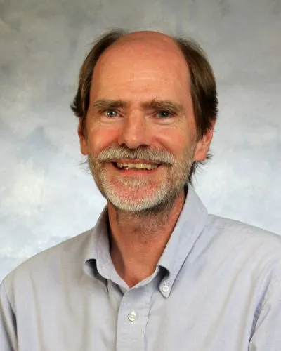
Dr. John Lindsey
Teaching Professor College of Engineering & Applied Science
ENGR 226
ENGR 226
Biographical Sketch
Dr. Lindsey received the B.S. degree in Electrical Engineering from Columbia University in New York and the B.A. degree in History from Colorado College in 1983 through the 3-2 combined plan. He then worked as a process engineer in the microelectronics and MEMS industries in the USA and Japan. In 1994 he entered graduate school at UCCS receiving the Ph.D. in Electrical Engineering in 1999 while continuing to work full-time. From 2007 Dr. Lindsey taught courses as a lecturer at UCCS as his work focus changed to high-frequency hybrid package development and manufacturing. He joined the faculty as an instructor in the fall of 2014.
Dr. Lindsey began at Inmos Corp, Colorado Springs as a photolithography/etch process engineer, helping manufacture some of the first high-performance, all-stepper, all-implant 16k SRAM and 64k DRAM chips with 1.8 _m minimum dimensions. He gained on-the-job experience with Statistical Process Control (SPC) and Statistical Design of Experiments (DOE), as well as participating in the steady changes Moore’s Law brought transitioning to 1.6 _m 64k SRAMs and 0.8 _m processing of 256k SRAMs. Following Inmos, he helped startup a 1 Mbit DRAM line at Motorola in Mesa Arizona, and then moved to Japan working for Ramtron/United Memories at NMB Semiconductor.
Working in two of NMB Semiconductor’s highly automated fabs, Dr. Lindsey developed photolithography processes down to 0.5_m and evaluated multiple generations of steppers and coat-develop tracks for high volume manufacturing of 1Mb, 4Mb and 16Mb DRAMs. Dr. Lindsey learned Japanese language, manufacturing methods, and adapted to the culture while working in Japan.
Returning from Japan in 1993, Dr. Lindsey moved to Ford Microelectronics as a research and development engineer developing photolithography and etch process for manufacturing MicroElectro-Mechanical (MEMS) accelerometers for airbags. While at Ford, he directed all aspects of one of the earliest deep silicon etch projects (DRIE) pioneering the first cryogenically-cooled, switched-gas (“Bosch Process”) ICP etcher in the world.
After the closure of Ford (Visteon) and receiving his Ph.D. from UCCS, Dr. Lindsey worked in Japan for Agilent Technologies at Agilent Labs Japan and in Colorado at the Colorado Springs Technology Center (CSTC) developing a MEMS liquid metal microswitch. He managed various project aspects and led development of wafer bonds with Cytop (a Teflon-like polymer); developed nano-liter liquid metal dispensing; investigated liquid metal properties, chemical reactions and reliability and simulated RF performance. Later Dr. Lindsey developed high-performance RF MCM products, processes and manufacturing at Agilent.
Research Interest
Dr. Lindsey’s research interests include liquid metal properties and applications to micro-switching; low energy electronic devices and design; solar cell devices.
Patents and Publications
- US patent 5920013, “Silicon micromachine with sacrificial pedestal”
- US patent 6646527, “High frequency attenuator using liquid metal micro switches”
- US patent 6747222, “Feature formation in a nonphotoimagable material and switch incorporating same”
- US patent 6774325, “Reducing oxides on a switching fluid in a fluid-based switch”
- US patent 6924443, “Reducing oxides on a switching fluid in a fluid-based switch”
- US patent 6979789, “Switches having wettable surfaces comprising a material that does not form alloys with a switching fluid, and method of making same”
- US patent 6995329, “Switch, with lid mounted on a thickfilm dielectric”
- US patent 7071432, “Reduction of oxides in a fluid-based switch”
- John R. Lindsey, T.S. Kalkur, “Capacitance voltage characteristics of polysilicon-polysilicon oxide-polysilicon structures for three-dimensional memory” MRS Proceedings Volume 609, Spring MRS meeting 2000, San Francisco, CA, April 24-28, 2000”
- John R. Lindsey, T.S. Kalkur, “Polysilicon Thin Film Transistor and EEPROM Characteristics for Three Dimensional Memory," 198th Meeting of The Electrochemical Society, Phoenix AZ, Oct 22-27, 2000”
- T.S. Kalkur, John Lindsey, “Electrical characteristics of Pt-SBT-Polysilicon (MFIP) capacitors with yttrium oxide as the buffer layer,” Integrated Ferroelectrics, Volume 34, Issue 1 – Feb 4, 2001 , pages 147 - 153